By Alibaba Cloud Storage Team
In Part 1 of the article series, we briefly discussed the evolution of storage media and then discussed in depth the technology and hardware of non-volatile memory express solid-state drives (NVMe SSDs). In Part 2, we will be analyzing the performance factors for NVMe SSDs.
The performance data provided by the NVMe SSD vendor specification is perfect. The performance comparison between the NVMe SSD and a common disk shows that NVMe SSD performance is indeed much better than disk performance. In the actual application, however, NVMe SSD performance may not be as good as expected, and it seems that the performance is not stable. The rules that make perfect NVMe SSD performance have not been found. Compared to a common disk, SSD performance is affected by many factors. To analyze SSD performance factors, we need to first understand the main parts of an SSD. As shown in the following figure, an SSD includes the following parts: host CPU, PCIe interconnection bandwidth, SSD controller and FTL software, backend NAND flash bandwidth, and NAND flash medium. The main factors affecting SSD performance can be divided into hardware, software, and other objective factors.
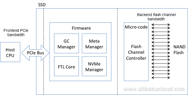
NAND flash
Different types of NAND flash have different performance. For example, the performance of SLC is better than that of MLC, and the performance of MLC is better than that of TLC. SSDs employing different types of NAND flash have different performance.
The count of backend channels (CE count) and bus frequency
The count of backend channels determines the count of concurrent NAND flash memories. Different SSD controllers support different channel counts. Therefore, the SSD controller type determines the backend throughput bandwidth of an SSD. The bus frequency of NAND flash channels also determines the access performance.
Processing capability of the SSD controller
The SSD controller runs complex FTL processing logic to convert read and write requests of logical blocks into NAND flash read and write requests. The requirements on the processing capability of the SSD controller are not high when data is read from or written to large blocks, but extremely high when data is read from or written to small blocks. The processing capability of the SSD controller is prone to be a performance bottleneck for the entire I/O system.
Architecture of the SSD controller
Generally, the SSD controller uses the symmetric multiprocessing (SMP) or massively parallel processing (MPP) architecture. Early controllers usually use the MPP architecture. In the MPP architecture, multiple small processors interconnect through the internal high-speed bus and communicate through the hardware message queue. Memory resources are used as separate peripherals shared by all processors. This architecture is similar to a distributed system based on message communication. The MPP architecture has a great advantage in performance, but its programming is complex. The performance scalability of the SMP architecture depends on software and its programming is as simple as that on an x86 server. The controller architecture affects the overall SSD performance. In the SSD design, we need to select different types of SSD controllers based on design goals.
Memory capacity
For better performance, the resource mapping table inside the SSD resides in the memory. The memory space occupied by the table is 0.1% of the SSD capacity. Insufficient memory capacity may cause mapping table swap-in and swap-out issues, affecting performance.
PCIe throughput bandwidth
The PCIe frontend bandwidth reflects the frontend throughput of the SSD. Currently, the NVMe SSD uses the x4 lane access mode and the maximum bandwidth allowed is 3 Gbit/s. The frontend PCIe tends to be a performance bottleneck when the backend NAND flash bandwidth and processor capability are sufficient. The NAND flash has high read performance. The read performance of an SSD is greatly limited by the PCIe bus. Therefore, the PCIe 4.0 standard needs to be rapidly advanced.
Temperature
If the NAND flash runs at full speed, a large amount of heat dissipation occurs. When the temperature rises to a certain value, the system becomes abnormal. To resolve this issue, the SSD has a temperature control system. This system monitors the temperature and adjusts SSD performance accordingly to keep the system temperature within a specified threshold. Essentially, SSD performance is compromised to reduce the temperature. Excessive high ambient temperature affects SSD performance and triggers the internal temperature control system to adjust SSD performance.
Service life
The probability of bit errors rises as the NAND flash is continuously erased and reused, resulting in the deterioration of SSD I/O performance.
Data layout
The data layout design needs to take into account concurrent units in the NAND flash, that is, how to convert I/O operations into concurrent operations of the NAND flash. For example, data layout is arranged on a multi-channel page by means of data interleaving. In this way, the sequential bandwidth can be optimized.
Dispatching during GC and wear leveling
Operations such as GC, wear leveling, and data retention result in a large amount of NAND flash backend traffic. The backend traffic directly reflects the write amplification factor of the SSD and the backend bandwidth consumption. The backend traffic generated can also be called background traffic, which directly affects the frontend performance. Therefore, the background traffic and user traffic need to be properly dispatched to achieve optimal I/O performance for users.
Overprovisioning (OP)
To resolve issues such as damaged blocks and GC, some spare resources are reserved inside the SSD. These reserved resources are also called overprovisioned resources (OP resources). More OP resources indicate less data moved during GC on average and less background traffic, which reduces the write amplification and improves user I/O performance. On the contrary, if fewer OP resources are reserved, the performance deteriorates and the write amplification increases. When the capacity of SSDs is small, a larger OP value is often specified to prolong the service life of an SSD.
Bit error
The following mechanisms are used inside the SSD to correct bit errors generated by the NAND flash: ECC, read retry, soft LDPC, and RAIN. When the bit error rate increases, software processing overhead also increases. However, if the bit error rate is controlled within a certain range, the errors can be corrected by the hardware. When software is involved in bit error correction, performance overhead becomes greater.
FTL algorithm
The FTL algorithm affects SSD performance. The FTL design and implementation vary depending on the application purpose of an SSD. Enterprise-oriented SSDs usually apply flat mapping and cache mapping tables consuming much memory space to ensure high performance. Consumer-oriented SSDs usually apply layered storage through metadata swap-in and swap-out based on pSLC+TLC to reduce cost. They can also cache metadata in the host memory space to reduce cost. These two methods, however, both affect performance.
I/O scheduling algorithm
The NAND flash has severe performance asymmetry, with millisecond-level erase and program latency and microsecond-level read latency. Consequently, how to schedule erase, program, and read operations needs to be considered during SSD backend design. In addition, the frontend I/O and backend I/O also need to be considered, and optimal performance can be achieved through I/O scheduling. In the I/O scheduling process, it is also necessary to take advantage of NAND flash features, such as program suspension, to achieve optimal SSD frontend I/O performance.
Driver software
The driver software runs on the host in kernel mode or user mode. In kernel mode, the software consumes more CPU resources and encounters frequent context switching and interruptions, so the performance is low. In user mode, the software usually uses the I/O polling mode to avoid context switching to fully improve the CPU efficiency and overall I/O performance.
I/O pattern
The I/O pattern affects the GC data layout inside the SSD, which indirectly affects the amount of data moved during the GC process and determines the backend traffic. The full sequential I/O pattern is the friendliest pattern for GC in the SSD. When an SSD uses the full sequential I/O pattern, the write amplification is close to 1 and the SSD achieves optimal performance. When an SSD uses the small block-based random I/O pattern, more data records are moved during GC and performance is significantly reduced. In practical applications, the I/O pattern needs to be optimized through the local file system to achieve optimal performance.
SSD use time
After being used for a long time, the wear of the NAND flash inside the SSD becomes worse and the bit error rate increases. There is a complete bit error recovery mechanism inside the SSD, which involves both hardware and software. When the bit error rate reaches a certain degree, the hardware mechanism fails, and software (firmware) needs to be used to restore flipped bits. However, the software mechanism causes great latency, which affects SSD performance. In some cases, SSD performance may deteriorate after the SSD is powered off for a period because a charge leakage fault has occurred on the SSD NAND flash during this period. As a result, the bit error rate increases. SSD performance is time dependent and it is essentially related to the bit error rate of the NAND flash.
Ambient temperature
The SSD has a negative feedback mechanism designed to restrict the temperature within a proper range. Based on the detected temperature, this mechanism adjusts the backend bandwidth of the NAND flash to reduce the SSD temperature. If the mechanism starts to work, the NAND flash backend bandwidth is limited, which affects I/O performance of the frontend application.
The following sections describe the impact of GC and I/O patterns on SSD performance from a software perspective.
The SSD has a very heavy software layer inside. This layer is used to resolve NAND flash issues and it records data in log-structured mode. However, the log-structured mode introduces the Garbage Collection (GC) issue. For frontend business, GC traffic is background noise. GC traffic does not exist all the time, so SSD performance greatly fluctuates. When the SSD is empty, its performance is optimal. After the SSD is used for a period, its performance greatly deteriorates. In this process, GC plays an important role. The specification released with an enterprise-oriented SSD provides the steady-state performance indicators of the SSD. During the performance test, SSD aging needs to be pre-processed. During the pre-processing, sequential data is written to the full SSD and then random data is written to the SSD twice. After the pre-processing, a random read/write test is conducted on the SSD to obtain the steady-state performance values provided by the specification. The steady-state performance values can be considered the minimum performance values of the SSD.
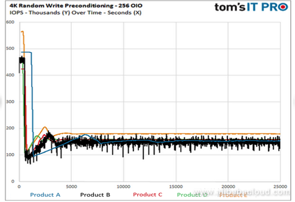
The above figure shows the performance comparison of multiple vendors' SSDs in the empty and steady statuses. The difference between the performance in the steady status and empty status is huge. In the steady status, GC inside the SSD is performed at full speed, which occupies a lot of NAND flash backend bandwidth. The ratio of the background traffic to the frontend traffic reflects the write amplification factor of the SSD. The larger the write amplification factor, the more bandwidth the background traffic occupies and the worse the SSD frontend performance is. The write amplification factor is affected by many factors, such as OP and application I/O pattern. A better application I/O pattern reduces the write amplification factor and background noise, and improves the performance of frontend business. For example, if data is written into an SSD in full sequential mode, the write amplification factor is close to 1 and data traffic generated by GC is little (almost no background traffic generated). The backend bandwidth is almost fully occupied by business data traffic, so SSD performance is perfect.
GC is an important factor affecting SSD performance. In addition, GC leads to increasing write amplification and shortens the SSD service life. From a software perspective, we can optimize the I/O pattern to optimize the SSD internal GC to further improve SSD performance and prolong the service life. We should apply this optimization method to the next-generation of cheaper QLC SSDs so they can fully meet the actual business application requirements.
The I/O pattern has a serious impact on SSD performance mainly in the following aspects:
When designing a flash memory system, we need to consider the impact of the I/O pattern on system performance. We can optimize system performance through software optimization. In practical use, the full sequential I/O pattern is seldom used except for writing logs. We will be convinced that the sequential pattern can optimize SSD performance if we have an in-depth understanding of the SSD. Once we know the implementation logic inside an SSD, we can try to use an appropriate method to realize sequential write as much as possible to achieve optimal SSD performance.
The SSD records data in log-structured mode. The concurrently written I/O data is aggregated into large data blocks in chronological order. The large data blocks are then written into the NAND flash as page stripes. Multiple page stripes are written into the same GC unit (chunk or superblock). When a GC unit is full, it enters the sealed mode (read-only). Then, a new GC unit is allocated for writing subsequent data. If multiple applications concurrently write random data into an SSD in this mode, the data of these applications is interleaved and stored in the same GC unit. As shown in the following figure, the data lifecycle varies according to the application. When a GC unit needs to be recycled, a large amount of data is migrated, which causes write amplification and affects SSD performance and service life.
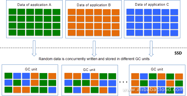
As above mentioned, the data records of different applications may be interleaved and stored in the same GC unit. This issue is essentially due to the interleaved storage of data of different hot and cold levels. For GC, it is best to store cold or hot data of the same level in the same GC unit. For this reason, Samsung launched the multi-stream SSD, which allows data from different applications to be stored in different stream units (GC units), thereby improving GC efficiency and reducing write amplification. The multi-stream SSD uses an explicit design that requires changes to the SSD interfaces and applications. We can achieve a similar effect by writing large blocks in the sequential I/O pattern. Suppose there is only one thread in the SSD and all applications use large data blocks to write data. In a time segment, only one application writes data into the SSD. In this way, the data stored in a GC unit becomes sequential and regular. As shown in the following figure, the cold or hot data of the same level is stored in the same GC unit after the above mentioned method is used. The data migrated during GC is greatly reduced, and the background traffic is reduced accordingly.
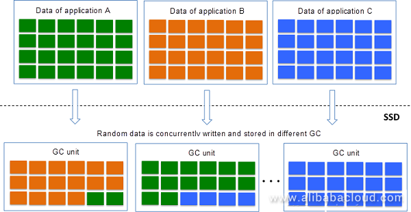
In practical use, the above I/O pattern is difficult to use because applications seldom generate extremely large grained requests. For this reason, we can use the high-performance Optane memory as the write cache of the SSD when designing the storage system. Write requests from different frontend applications are first written into the Optane persistent medium and aggregated into large data blocks in the medium. The large data blocks are then written into the SSD. In this way, sequential write can be achieved as much as possible to improve SSD performance and service life.
As shown in the following figure, the NAND flash has a serious read/write asymmetry. The block erase and page program latency can be much longer than the page read time. If the read operation conflicts with the erase or program operation on the same flash channel, the read operation is affected by the erase or program operation. This is an important factor affecting the read performance when the read and write operations are mixed.
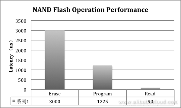
In practical use, it is often found that the application test results do not match the values provided by the SSD specification, and the actual values are smaller than the values provided by the specification. The performance indicator values provided by the specification are usually calculated in the case of pure read or pure write operations. When the read and write operations are mixed, the actual values are significantly different from the values provided by the specification.
Test results show that there is a large performance gap between different SSDs when the read and write operations are mixed. When SSDs are in the steady status and applications use the random read pattern, you can find that the SSDs have different anti-disturb capabilities when a small amount of data is transferred in sequential write. In the case of write disturb, the read performance of some SSDs drops dramatically, the latency rises rapidly, and the QoS cannot be guaranteed. The following figure shows the test results of two different SSDs in the same situations. The results show that different SSDs have different anti-disturb capabilities. The read performance of SSDs that have a strong anti-write disturb capability does not drop dramatically.
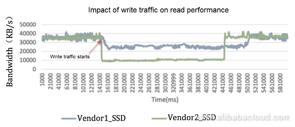
Why do some SSDs have a strong anti-write disturb capability? The mystery lies in the I/O scheduler inside the SSD. The I/O scheduler schedules the write, read, and erase requests. SSDs using different scheduler algorithms have different anti-disturb capabilities. At present, many NAND flash memories support the program or erase suspension function. In the I/O scheduling process, the Suspension command can be used to suspend the program or erase requests so that read requests can be scheduled first. This reduces the read request latency to improve the read performance.
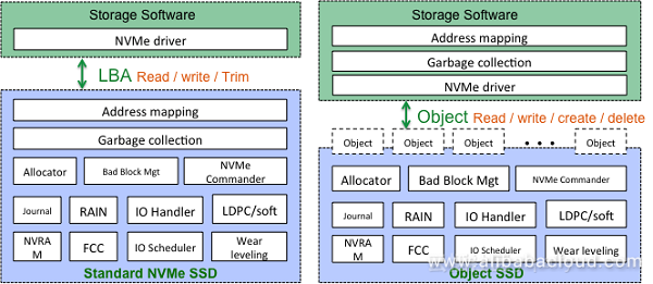
The read-write conflict is an important factor affecting the I/O QoS within SSDs. The SSD QoS can be improved through optimization of the I/O scheduler, but it is still not possible to optimize the SSD QoS through cooperation with the storage software. To achieve optimal SSD performance and QoS, we need to use open-channel technology. Open-channel is actually just a method of hierarchically dividing hardware and software. Generally speaking, the logic inside the SSD can be divided into the physical resource management layer for NAND resources and the resource mapping layer oriented to the data layout. Physical resource management can be placed inside the SSD because it is closely related to the NAND flash. The traditional NVMe SSD needs to expose the standard block device interface, so the resource mapping layer needs to be implemented inside the SSD. From an end-to-end perspective, the resource mapping layer can be combined with the storage software layer. For this purpose, the resource mapping layer is stripped from the inside of the SSD and integrated into the storage software layer. Once the resource mapping layer is stripped from the inside of the SSD, a new SSD interface needs to be defined. Open-channel is one of these interface modes.
We have done a lot of researches on SSD QoS in Apsara Distributed File System and put forward the concept of Object SSD, which is a new SSD interface mode. We use the object mode to read data from and write data into an SSD. Each object uses the append write operation mode. In this mode, the interface can be seamlessly integrated with Apsara Distributed File System. With Object SSD, a lot of work within the SSD is simplified, I/O scheduling is more flexible, and the storage software cooperates with the SSD to optimize I/O performance and maximize the QoS.
The data traffic inside the SSD is divided into two categories: frontend user data traffic and internal background data traffic. The frontend user data traffic and the background data traffic are aggregated into the NAND flash backend traffic. When there is no background data traffic, the NAND flash bandwidth is fully occupied by the user data traffic. In this case, SSD performance is optimal. When the SSD has a large write amplification, it produces a large amount of background data traffic, which occupies the NAND flash bandwidth, resulting in deterioration of the frontend user I/O performance. To stabilize the frontend I/O performance, the scheduler inside the SSD balances the frontend and background data traffic to ensure frontend performance consistency. The proportion of background data traffic reflects the write amplification factor of the SSD. From the perspective of the NAND flash bandwidth occupation, we can analyze the performance of the SSD in the steady status.
Suppose the write amplification factor is WA, the total bandwidth occupied by sequential write is B, and the user data write traffic (random write traffic) is U. Then, the background data traffic caused by GC write amplification is: (WA - 1) x U
Both read and write operations occupy bandwidth. Therefore, the total bandwidth occupied is calculated as follows:
B = 2 x (WA - 1) x U + U
Then, we can get:
U = B/[2 x (WA - 1) + 1] = B/(2 x WA - 1)
The above formula expresses the relationship between the frontend user data traffic, the total NAND flash bandwidth, and the write amplification factor.
According to the specification, the sequential write bandwidth of Intel P4500 is 1.9 Gbit/s. Based on the above formula, the frontend user data traffic in random access mode is: 1900/(2 x 4 - 1) = 270 Mbit/s. The IOPS is 67 KB. The result is consistent with that provided by the specification.
The following figure shows the comparison between the random write latency of Intel P4500 and Samsung PM963 and the values derived from the formula. The results are consistent.
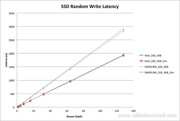
Based on this, we can infer that the random write performance is determined by both the SSD backend bandwidth and the write amplification factor. Therefore, from the perspective of storage software, we can optimize the I/O pattern to reduce the write amplification factor and improve the random write performance of the SSD.
Flash storage technology is rapidly developing. Centered on flash storage, the flash media, SSD controller, storage system software, and storage hardware platform are all evolving. The value that flash memory brings to data storage is obvious. The use of flash memory in IDCs is a trend. NVMe SSD performance is affected by many factors. At the software level, we can optimize the I/O pattern to improve the performance of the SSD and the overall storage system.
Storage System Design Analysis: Factors Affecting NVMe SSD Performance (1)

2,593 posts | 793 followers
FollowAlibaba Clouder - January 15, 2019
Alibaba Clouder - August 13, 2019
ApsaraDB - December 26, 2023
Alibaba Clouder - July 5, 2018
Alibaba Clouder - March 21, 2018
Alibaba Cloud Community - April 25, 2022

2,593 posts | 793 followers
Follow OSS(Object Storage Service)
An encrypted and secure cloud storage service which stores, processes and accesses massive amounts of data from anywhere in the world
Learn More Apsara File Storage NAS
Simple, scalable, on-demand and reliable network attached storage for use with ECS instances, HPC and Container Service.
Learn MoreMore Posts by Alibaba Clouder
Raja_KT March 14, 2019 at 11:34 am
Interesting...one.... " We use the object mode to read data from and write data into an SSD. Each object uses the append write operation mode. In this mode, the interface can be seamlessly integrated with Apsara Distributed File System. With Object SSD, a lot of work within the SSD is simplified, I/O scheduling is more flexible, and the storage software cooperates with the SSD to optimize I/O performance and maximize the QoS."