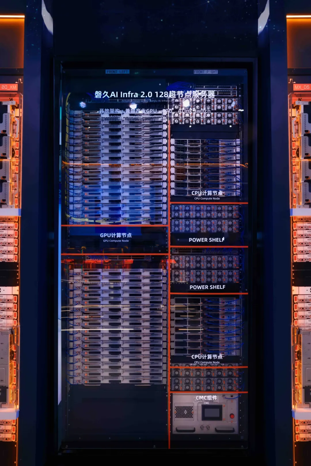
At the Apsara Conference 2025, Alibaba Cloud unveiled its new-generation Panjiu AI Infra 2.0 AL128 supernode AI servers.
As supernode AI servers, Panjiu AL128 adopts a service architecture designed for next-generation ultra-large clusters and reconstructs the interconnect mode between GPUs. It aims to achieve optimal collaboration between computing power and communication in foundation model training and inference scenarios. Compared with traditional architectures, the architecture of Panjiu AL128 can improve inference performance by 50% based on the same AI computing power.
This article analyzes Panjiu AL128 supernode AI servers and their interconnect architecture to discuss what supernode servers are, how GPUs are efficiently interconnected for supernode servers, and how supernode servers drive the evolution of AI computing technologies.
Foundation model training involves models at large and increasing scales, large amounts of diversified data, intensive and time-consuming computing, and a huge amount of computing resources. It requires extremely high computing power, throughput, and precision. The training process pursues fast convergence and timeliness. Therefore, the core requirements for AI servers are larger computing scales, more cache capacity, and higher communication bandwidth.
Foundation model inference requires a specific amount of highly discrete data for a single inference and balanced computing power and cache capacity. Especially in the prefill-decode disaggregation architecture, the required ratio of computing power to cache varies in different phases. The inference process pursues quick response and good user experience, and requires lower inference costs. Therefore, the core requirements for AI servers are large single-domain computing scales, flexible cache ratios, and lower communication latency.
As the competition of foundation models enters the model inference phase, various foundation model inference tools, AI assistants, multimodal content understanding and generation tools, and video generation tools emerge one after another. During this period, the design of AI servers must pay more attention to the following demands of foundation model inference: single-domain computing power, low-latency communication, flexible ratio of computing power to cache, and higher cost-effectiveness.
These factors are both interdependent and mutually restrictive. The computing power and cache size can be adjusted on GPUs. However, during foundation model inference, the requirements for computing power density and cache capacity vary based on the scenario and computing phase.
• Video generation by using Wan models requires higher computing power density and moderate cache capacity.
• For Qwen mixture-of-experts (MoE) models that use prefill-decode disaggregation, the prefill phase is computing power-intensive and does not require high cache capacity, whereas the decode phase requires higher cache capacity and bandwidth.
• Key-value (KV) caches trade cache space for computing time to reduce computing. As the number of KV caches grows, KV cache access must be optimized. This will be discussed later in the design of general-purpose computing supernodes.
Therefore, the design of AI servers must also consider heterogeneous GPUs and the use of heterogeneous GPUs for different scenarios and nodes. In this case, inter-GPU communication requires higher bandwidth and lower latency. Under the conditions of ever-increasing model scales and computing power demands, due to the limited computing power and cache capacity of a single chip, the core challenge in designing foundation model training and inference servers lies in chip interconnection, specifically the interconnection of supernode servers.
This section starts with the hardware system of a Panjiu AI Infra 2.0 AL128 supernode AI server.
• Customized double-wide rack: A rack supports 128 to 144 GPUs, up to 350 kW power supply capacity and 500 kW heat dissipation capacity, and 2 kW heat dissipation capacity by using liquid cooling for a single GPU. It uses busbars for centralized power supply.
• Flexible modular and multi-dimensional decoupling system architecture: The system decouples CPU nodes from GPU nodes, decouples GPU nodes from ALink Switch nodes, and decouples compute nodes from power supply nodes. This architecture is not only compatible with mainstream CPUs, GPUs, and ALink Switch chips in the industry, but also supports the independent evolution of major chips and the flexible ratios of CPUs to GPUs.
• Orthogonal interconnection between GPU nodes and ALink Switch nodes: The orthogonal interconnect architecture uses high-speed connections to minimize loss and reduces complex cabling and coupling. This improves system reliability and O&M performance. The architecture also shrinks the granularity of field replaceable units (FRUs) from the rack level to the node level, and shortens the FRU replacement duration from hours to minutes.
• Single-stage interconnect architecture and non-Ethernet ALink protocol: The system supports UALink, an international open standard, and also supports interconnect protocols for the native memory semantics of mainstream GPUs in the industry, such as NVLink, xLink, UB, and xCN.
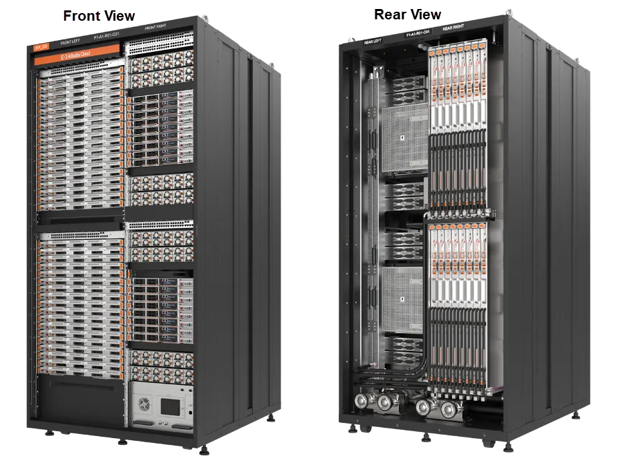
Figure: Front view and rear view of a Panjiu AL128 supernode AI server
From the front view of the rack, GPU nodes and ALink Switch nodes are deployed in the orthogonal interconnect architecture on the left side of the supernode, which consists of the upper and lower ScaleUp domains, each with a group of AL64 GPUs. A ScaleUp domain with a group of AL128 GPUs will be supported later. The orthogonal interconnect architecture enables the extremely low loss of high-speed connections, 112 Gbit/s or 224 Gbit/s Serializer/Deserializer (SerDes) for GPUs and ALink Switch chips, and higher system reliability.
CPU nodes and power supply nodes are deployed on the right side of the supernode. In this separate deployment mode, CPU nodes and GPU nodes can be flexibly configured, such as 8, 16, or 32 GPUs for a single OS. In addition, CPU nodes and GPU nodes across platforms and generations can be flexibly combined to support heterogeneous GPUs.
Then, how are Panjiu supernode AI servers interconnected?
In model inference scenarios, large language models (LLMs) use a large number of parameters, such as more than 1 trillion parameters for the Qwen3-max model. A single inference task can be run on 8 to 32 GPUs. However, considering the development trends of large-scale expert parallelism (EP) and the storage requirements of long sessions for KV caches, 32 to 128 GPUs can provide better user experience.
Video generation models such as Sora2 and Wan2.2 use the DiT diffusion model, which does not use a large number of parameters but requires higher computing power. In this case, 32 GPUs can support high parallelization acceleration. To meet the demands of cloud computing for resource scheduling and flexibility, a supernode with 64 to 128 interconnected AI chips can meet the requirements of most inference applications in the next three years.
The interconnection of supernode servers can further support a larger-scale network topology based on layered interconnection, providing more flexible and elastic resource scheduling, and also supporting model training scenarios in large-scale clusters. Panjiu AI Infra 2.0 supernode AI servers support a three-layer interconnect architecture. At Layer 1, GPUs are interconnected in each ScaleUp domain of a supernode. At Layer 2, supernodes are interconnected to form a ScaleOut network. At Layer 3, supernodes and data centers are interconnected to establish a data communication network (DCN).
From the front view of a Panjiu supernode AI server, the upper-left section is a ScaleUp domain that contains 64 to 72 GPUs and consists of 16 to 17 GPU nodes at the front and eight ALink Switch nodes at the rear. Each GPU node has four GPUs, and each ALink Switch node has multiple ALink Switch chips. In this case, 64 to 72 GPUs in a ScaleUp domain can be connected in non-blocking full-interconnect mode in the single-stage switching topology.
The following figure shows the topology of ScaleUp interconnection within a supernode. In this example, ALink Switch chips with 64 ports are used. Each ALink Switch node has one or two ALink Switch chips, and 16 GPU nodes have a total of 64 GPUs. ScaleUp ports 0 and 8 of each GPU are connected to the ALink Switch chips on the ALink Switch 0 node by using orthogonal connectors. ScaleUp ports 1 and 9 of each GPU are connected to the ALink Switch chips on the ALink Switch 1 node by using orthogonal connectors. The rest ports of each GPU are connected to the ALink Switch chips on other ALink Switch nodes in the same way. Two groups of AL64 GPUs in the upper and lower ScaleUp domains support cross-domain connections. However, under the principle of single-stage switching, ALink Switch chips with 128 ports are required.
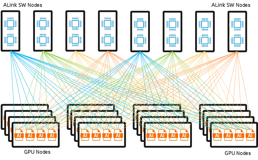
Figure: Topology of ScaleUp interconnection within a Panjiu supernode AI server
The architecture of ScaleUp interconnection within a supernode reserves a maximum of 128 high-speed interconnected SerDes for each GPU, with a maximum interconnect bandwidth of 14 Tbit/s to 28 Tbit/s per GPU. The single-stage switching topology is used to take advantage of the extremely low latency of ScaleUp interconnection and shorten the duration of inference tasks. This topology is also in line with the ALink protocol for the native memory semantics of GPUs. Based on minimalist communication protocols, ScaleUp interconnection obtains extremely low data communication latency, reduces the end-to-end latency of single inference tasks, and improves user experience during foundation model inference.
As the dimension with the highest bandwidth among the three interconnect dimensions, ScaleUp interconnection raises the following requirements that are natively designed for modern GPUs, based on the AI traffic patterns it faces, ultimate performance requirements, and implementation challenges:
• Native memory semantics: supports direct access to the computing cores of GPUs and simplifies the interface with the system on a chip (SoC) bus, without translation overhead or intrusive modifications to the computing cores.
• Ultimate performance: achieves extremely high bandwidth (up to TB/s per chip) and ultra-low latency. This is made possible not only by the high packet efficiency of protocols but also by exceptional performance under heavy loads.
• Minimalist implementation: minimizes the resource overhead of chips by employing the smallest chip area, reserving valuable resources and power for the computing power and on-chip storage of GPUs.
• High-reliability connection: ensures high availability by using a high-performance physical layer, coupled with the retransmission and fault isolation mechanisms in environments with high-density SerDes.
The ScaleUp interconnect protocols of mainstream GPUs in the industry are all based on the first principle of GPU computing and meet the preceding requirements by using technologies such as flow control units (flits), LLC, and credit-based flow control (CBFC). The international open standard UALink and high-efficiency GPU interconnect protocols such as NVIDIA NVLink, Ascend UB, and AMD xCN all adopt similar technologies as the foundation for ScaleUp interconnection. These protocols use an independent data-link layer and upper-layer formats, rather than Ethernet protocols.
An ironic industry trend has emerged in recent years. Protocols such as UEC, SUE, and ETH+, which are intended for ScaleUp interconnection, have successively abandoned the Ethernet frame format and even modified the Ethernet preamble. They do this to achieve technical effects similar to those of the GPU-native ALink protocol. Although they are still touted as Ethernet, they are incompatible with standard Ethernet protocols and lack the concept of IP addresses. In essence, they are no longer Ethernet protocols.
Ultimately, technological competition within the industry is beneficial for its development, and will accelerate the rapid innovation of AI interconnect networks. Therefore, these practices of significantly modifying and adapting Ethernet protocols offer valuable insights for the protocol iteration of ScaleOut between supernode servers, which will be discussed in detail later.
To support larger GPU interconnect clusters and cope with demands such as foundation model training and the flexible scheduling of computing resources, Panjiu supernode AI servers also support a ScaleOut network across supernodes.
Inside a GPU node, it has four high-performance network interface cards (NICs) in the front window, which can provide a ScaleOut network bandwidth of 400 Gbit/s to 800 Gbit/s for each GPU. In total, Panjiu supernode AI servers reserve a bandwidth of 25.6 Tbit/s to 51.2 Tbit/s for network communication between supernodes. A combination of ScaleUp and ScaleOut communication optimization technologies can provide a GPU-GPU communication bandwidth of at least 10 Tbit/s within supernodes and between supernodes. This ensures sufficient bandwidth for foundation model training and inference scenarios.
As mentioned earlier, protocols such as UEC, SUE, and ETH+ have abandoned the Ethernet frame format. Their practices of significantly modifying and adapting Ethernet protocols offer valuable insights for the protocol iteration of ScaleOut between supernode servers. Given that the scale of AI clusters is ultimately limited, even clusters with tens or hundreds of thousands of GPUs, combined with VM partitioning, may not require 48-bit MAC addresses. Perhaps 24-bit to 32-bit MAC addresses are sufficient.
Therefore, in the future, a ScaleOut network may not necessarily be based on Ethernet, and can adopt a more simplified protocol. GPUs use a ScaleOut network for data communication to exchange memory data between GPUs. In essence, data communication is still based on Remote Direct Memory Access (RDMA). Therefore, the RDMA over Converged Ethernet (RoCE) protocol currently used for ScaleOut must also be transformed for the exchange of GPU memory data. The splitting of ScaleOut network traffic will be discussed in detail later.
Foundation model training and inference are inseparable from data center networks. Data storage and interaction, such as user input, data retrieval over the Internet, training data, KV caches, and checkpoint-based backup, all rely on data center networks.
Panjiu supernode AI servers also provide interfaces to access data center networks. On each CPU node, a 400 Gbit/s to 800 Gbit/s intelligent NIC is integrated to provide GPUs with capabilities such as data storage, databases, data preprocessing, and data computing acceleration.
In general, the main value of supernode servers is manifested in AI model inference scenarios. In the next two to three years when the common number of model parameters reaches 10 trillion, each ScaleUp domain with about 128 GPUs on a supernode server can achieve an optimal balance between application performance and engineering implementation.
Foundation model inference scenarios are latency-sensitive. While the inference quality meets user expectations, users pay more attention to latency. Therefore, the ScaleUp interconnect protocol of supernode servers must focus more on communication latency while meeting the requirements for bandwidth design. ScaleUp interconnection uses the single-stage switching topology to maintain extremely low latency. The two-stage switching topology increases latency and therefore is of little significance. The scale of ScaleUp interconnection needs to meet the requirements of foundation model inference in the future. Each ScaleUp domain with 128 GPUs is the most cost-effective choice at present.
Traditional single-GPU and eight-GPU AI servers are designed based on a CPU-centric architecture. All GPUs are connected to CPUs over Peripheral Component Interconnect Express (PCIe), and then CPUs control NICs to complete data communication between GPUs and external data communication for GPUs.
In the era of supernode servers, changes are made to design servers based on a GPU-centric architecture. For example:
To increase the cache capacity and bandwidth of GPUs, CPUs and GPUs are interconnected over xLink C2C, instead of traditional PCIe.
To facilitate GPU access to RDMA networks, RDMA NICs are directly connected to GPUs.
However, the used technologies are still based on CPUs. For example, RDMA NICs are connected to GPUs over PCIe. To access SSDs, GPUs are connected to CPUs over PCIe. InfiniBand GPUDirect Async (IBGDA) is not natively designed for GPUs.
In the future, a GPU-centric interconnect architecture must be constructed for supernode AI servers. This section describes four research directions.
The industry has taken the first step to increase the bandwidth between CPUs and GPUs by using a chip-to-chip (C2C) protocol. For example, NVIDIA uses NVLINK C2C to connect CPUs to GPUs. The next step is to verify how to connect peripherals such as memory, NICs, and accelerators to GPUs.
The second direction is to reshape the access mode between GPUs and peripherals. Traditional peripherals, such as NICs, require complex control operations. The microarchitecture of CPUs is good at performing such drive control operations. However, these operations are very unfriendly to the single instruction, multiple threads (SIMT) architecture of GPUs and seriously waste the computing cores of GPUs. To meet the typical requirements of memory data exchange between GPUs, a ScaleUp Ultra card is designed to present the memory addresses and memory semantics of remote GPUs to local GPUs, enabling cross-domain address translation and data migration. Local GPUs need to only send data read and write requests to the memory addresses of remote GPUs by using simple memory semantics. The ScaleUp Ultra card is responsible for other complex operations such as driver control, address translation, and message encapsulation.
Traditional GPU clusters use the classic three-layer interconnect architecture: ScaleUp interconnection + ScaleOut network + DCN. At that time, a ScaleUp domain contains only 8 to 16 GPUs, and a cluster with tens of thousands of GPUs is built for training based on the ScaleOut network.
In the future, if the number of foundation model parameters exceeds 100 trillion, a ScaleUp domain of a supernode server must contain 256 to 512 GPUs. Most of the data communication can be complete within a ScaleUp domain, and the demand for cross-domain traffic on a ScaleOut network is reduced.
In addition, new topics are proposed for the interconnect architecture: After the bandwidth of DCN NICs multiplies from 400 Gbit/s to 1.6 Tbit/s, does the cross-domain traffic of supernode servers still need a ScaleOut network? Is it possible for the DCN to carry the cross-domain traffic? Of course, new topics bring more technical issues, such as the isolation of traditional DCN traffic from ScaleOut network traffic.
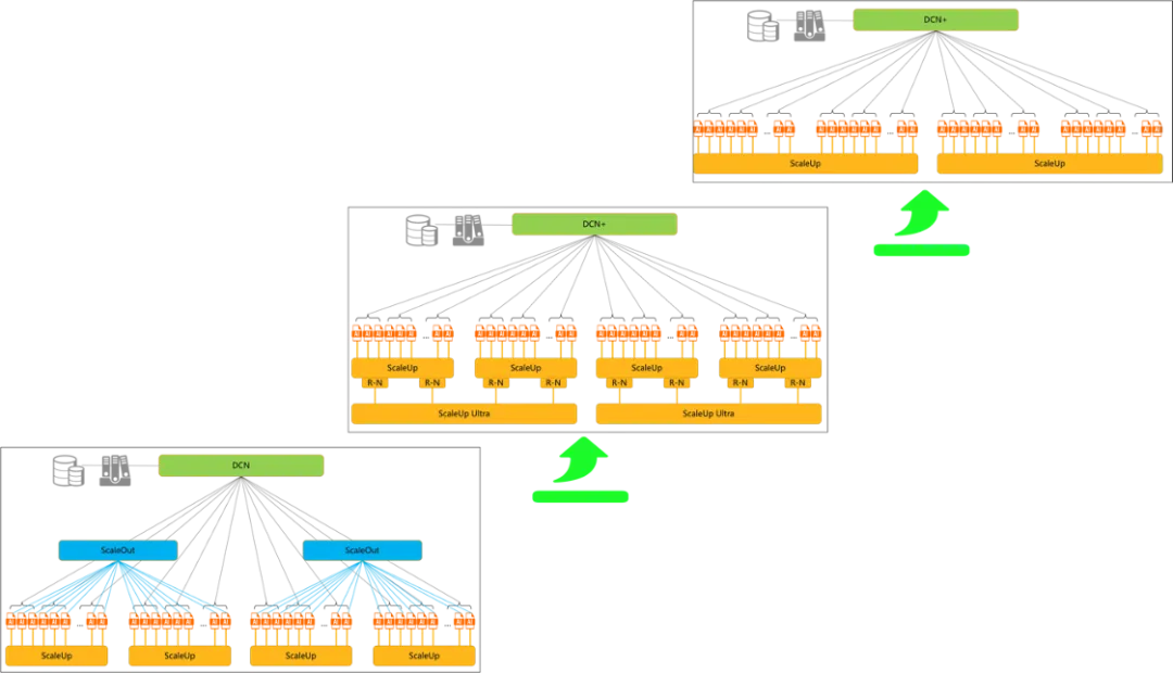
Figure: Simplified interconnect topology of supernode AI servers
To address new topics, a two-layer interconnect architecture is designed for supernode AI servers: ScaleUp interconnection + High-bandwidth DCN. The traffic to be carried by a ScaleOut network is split into two parts. One part of the traffic is carried by ScaleUp domains, and the other part of the traffic is carried by the high-bandwidth DCN.
The two-layer interconnect architecture not only simplifies the deployment of large-scale GPU clusters in a public cloud, but also reduces the base costs for the deployment of small-scale GPU clusters in a private cloud. If the scale of ScaleUp domains can meet the high bandwidth and low latency requirements of parallel computing such as tensor parallelism (TP) and EP, cross-domain traffic can be carried by the high-bandwidth DCN. Otherwise, the cross-domain communication capability of ScaleUp domains needs to be enhanced.
The communication data carried by a traditional ScaleOut network is the cache data exchanged between GPUs during RDMA communication. This exchange of cache data is similar to the exchange of GPU memory data in a ScaleUp domain, which also makes it possible for ScaleUp domains to carry part of the ScaleOut network traffic. Of course, a traditional ScaleOut network supports a more complex network topology and enhanced reliability, such as multi-path transmission, out-of-order reception, congestion control, and end-to-end reliable retransmission. If these technologies are directly integrated into the ScaleUp interconnect protocol, ScaleUp interconnection becomes more complex.
A feasible solution is to use the ScaleUp Ultra card mentioned earlier as a cross-domain GPU agent to implement data communication across ScaleUp domains. This also saves the computing power consumed by GPUs to perform operations on RDMA NICs when data is transmitted between GPUs over IBGDA. To formulate a protocol for data communication across ScaleUp domains, the ScaleUp interconnect protocol can be enhanced to integrate the ScaleUp Ultra card, the IB protocol can be used for reference, or cross-domain routing fields can be added to the ScaleUp interconnect protocol. Given that the number of nodes in GPU clusters is less than 100,000, Ethernet protocols that carry 48-bit MAC addresses are not necessary.
Optical interconnect technologies are popular in the past two years, such as linear-drive pluggable optics (LPO), near-packaged optics (NPO), and co-packaged optics (CPO), among which CPO attracts the most attention. Topics are raised to discuss whether the ScaleUp interconnection of supernode servers will use optical interconnect technologies, when to use optical interconnect technologies, and what technologies and modules to be used. This section discusses optical interconnection from the perspectives of the evolution of interconnect technologies for the ScaleUp interconnection of supernode servers and optical interconnect technologies.
The technical advantages of optical interconnection include high signal rates, low loss, and thin cables (facilitating cabling and O&M) for long-distance transmission. Wavelength division multiplexing can further reduce the number of optical fibers. However, the disadvantages of optical interconnection include high costs, high power consumption, and reduced reliability.
At present, a single rack with 128 GPUs is nearing its limits in terms of power supply, heat dissipation, and spatial layout. If model scales continue to increase and a ScaleUp domain of a supernode server contains 256 to 512 GPUs, cross-rack ScaleUp interconnection becomes inevitable. In addition, the ScaleUp bandwidth of AI chips continues to grow. When the SerDes rate slowly increases, the number of SerDes also increases for ScaleUp interconnection. Consequently, more cables and cable connectors are required, cables become thicker, and cabling and O&M are increasingly complex, leading to potential reliability risks.
Therefore, driven by long-term technological evolution, the ScaleUp interconnection of supernode servers will likely adopt optical interconnect technologies when a ScaleUp domain contains 256 GPUs, the SerDes rate hits 448 Gbit/s, and the end-to-end costs of optical interconnection become comparable with those of cables.
Optical interconnection supports multiple types of modules, including CPO, NPO, and LPO modules. The differences between these types of modules are not discussed in this article. From a hardware engineering perspective for supernode servers, NPO modules are preferred.
The following table compares the technical advantages and disadvantages of CPO, NPO, and LPO.
| Advantages | Disadvantages | |
|---|---|---|
| CPO | • Does not require printed circuit board (PCB) cabling, reducing the dependence of GPUs on 224 Gbit/s or 448 Gbit/s high-speed SerDes IP. • Makes full use of package space for cabling, saving layout space on PCBs. |
• Requires GPUs and Switch chips to integrate optical engines. This involves complex cooperation with different manufacturers, along with complex manufacturing, immature co-packaging technologies, and long implementation cycles. • Increases the GPU failure rate and the difficulty in plugging, unplugging, and maintaining optical fibers. |
| NPO | • Decouples optical interconnection from GPUs and Switch chips, allowing for more flexible optical technology iteration and supplier selection. • Enables short PCB cabling and low loss for high-speed SerDes. • Simplifies implementation, without intrusive modifications to GPUs and Switch chips. |
• Supports O&M only on boards, which is less convenient than panel-based O&M. • Occupies more layout space on PCBs. • Lacks unified industry standards and specifications. |
| LPO | • Uses existing technologies in a mature ecosystem and reduces the power consumption and costs of optical modules by removing digital signal processor (DSP) chips. • Simplifies O&M by allowing modules to be plugged and unplugged on panels. • Decouples optical interconnection from GPUs and Switch chips, without intrusive modifications to GPUs and Switch chips. |
• Provides large modules with low interface integration density, which cannot meet the high-density requirements of ScaleUp interconnection. • Requires long-distance PCB cabling from chips to panels, which makes it difficult to support the electrical signals of 224 Gbit/s or 448 Gbit/s high-speed SerDes. |
Optical interconnect technologies can bring more technical benefits to board-level engineering. For example, the use of retimer chips can be reduced to offset part of the costs of optical interconnection. Signal attenuation can be lowered, so that more efficient Reed-Solomon (RS) encoding can be used at the physical layer of the ScaleUp interconnect protocol to exchange for lower encoding latency, further reducing the latency of ScaleUp communication.
However, optical interconnect technologies still face more challenges in the ScaleUp interconnection of supernode servers. The first is reliability. The reliability of light is greatly related to temperature. Liquid cooling can be used to keep NPO modules and their light sources at a lower temperature, so as to obtain higher reliability. In addition, the seal design of optical connector interfaces must be improved to reduce the reliability risk caused by environmental dust. The second is maintainability. NPO modules, light sources, and optical connector interfaces must be pluggable to facilitate O&M in the event of failures and shorten the mean time to repair (MTTR).
Furthermore, the ScaleUp interconnect topology between GPUs and Switch chips is an interleaved mesh structure, which introduces the complexity of mesh connections for optical fibers, similar to the complexity of cable cartridges for cables. This results in a trap where a single optical fiber fault requires the replacement of the entire optical fiber group. This also needs to be cleverly avoided during engineering design.
Non-AI general-purpose computing scenarios require a flexible ratio of CPU computing power to memory. However, AI inference scenarios impose higher requirements for CPU compute nodes, especially memory-related features. In AI inference tasks, CPUs are responsible for data preprocessing and KV cache storage. Compared with regular computing tasks, AI inference tasks require larger memory capacity and higher memory bandwidth. Architecturally, AI applications require general-purpose computing supernodes to be interconnected to provide larger memory capacity and higher access bandwidth.
The architecture and computing tasks of CPUs are similar to those of GPUs but have unique requirements, which generally include:
• Memory semantics access: supports the load and store semantics initiated by CPUs, with the 64-byte cache line as the typical message length, allowing CPU cores to use extended memory without intrusive modifications.
• Extremely low latency: maintains a latency of hundreds of ns for CPUs to access Compute Express Link (CXL) memory, similar to the latency for CPUs to access local double data rate (DDR) memory, to meet the requirements of computing tasks on CPUs and minimize the requirements for cache resources on CPUs under memory extension.
• Data consistency: natively supports consistency protocols such as MESI between multiple CPU cores. This not only enables a series of hardware operations such as prefetch, but also enables task collaboration between multiple CPUs at the cache line level.
In the early days, the industry mainly relied on PCIe as the standard interconnect protocol between CPUs and peripherals such as accelerators. However, PCIe itself does not support cache coherency, resulting in the explicit management of data sharing between CPUs and devices, which increases software overhead and latency.
To resolve this issue, a series of protocols for CPU memory extension have emerged in the industry, including the OpenCAPI protocol launched by IBM, the CCIX protocol proposed by companies such as ARM, and the Gen Z protocol jointly promoted by several companies. After the CXL protocol emerges, the aforementioned protocols will eventually stop updating (for example, Gen Z transfers technologies to the CXL Consortium), or no longer be specific to memory extension (for example, CCIX focuses on dedicated CPU-CPU connections under the ARM architecture).
To this day, the CXL protocol has become the mainstream standard for CPU memory extension. It improves performance and reduces power consumption by providing a series of features such as memory semantics communication, allowing direct memory interaction between different components, and minimizing the involvement of applications or processors.
In the architecture that decouples computing from memory, node configurations become more modular. In addition to improved performance, this architecture also brings a range of benefits such as increased elasticity and flexibility, adding value to typical scenarios such as AI inference and PolarDB databases, including:
• Improved inference performance: Multiple CPU nodes with mounted GPUs share a CXL memory pool. This way, KV caches do not need data forwarding by host memory, shortening the data path. Synchronization between data transmission and data computing can be reduced, bypassing CPUs.
• Multi-node KV cache data sharing with easy feature extension: In scenarios where KV caches are hit, compared with an RDMA-based KV cache memory pool (such as MoonCake), the time to first token (TTFT) is reduced by 82.7% and the throughput is improved by 4.79 times.
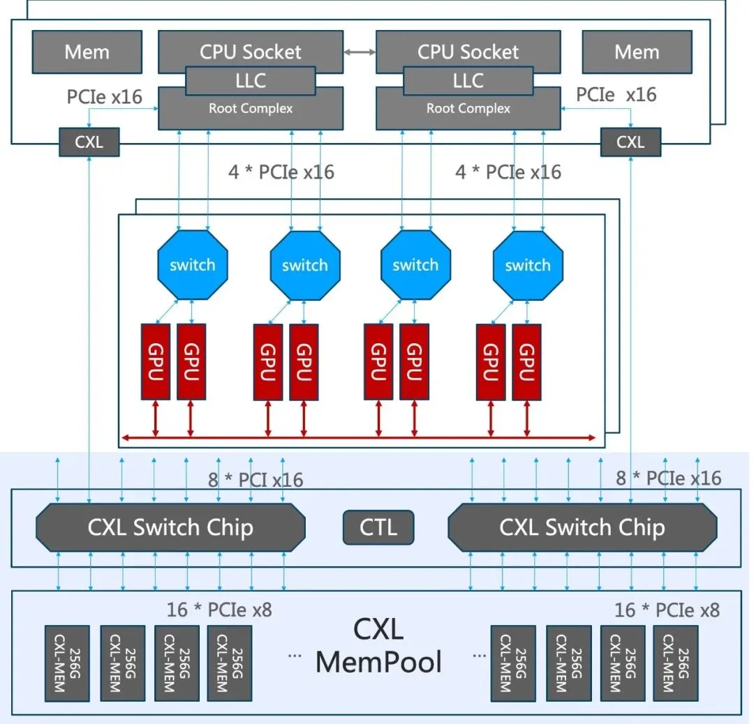
Figure: CXL-based interconnect architecture of general-purpose computing supernodes
Architecture evolution: CXL-based Panjiu supernode AI servers provide CPU nodes with a flexible memory pool with a latency of hundreds of ns, a bandwidth of hundreds of GB, and 10 TB-level memory capacity. A rack-level tiered memory solution is generated to provide applications with performance optimization and cost competitiveness based on a tiered memory architecture.
CPU general-purpose compute nodes, Switch nodes, and JBOM nodes are used to balance flexibility and high-performance memory extension.
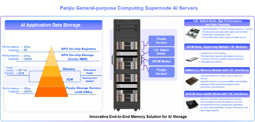
Figure: Innovative end-to-end memory solution for AI storage
Another technology trend stems from the memory I/O evolution of CPUs. The development of CPU chips faces challenges in I/O. One challenge is that the ratio of the memory access capability to CPU cores and computing power is increasingly difficult to meet the demands of various AI applications. The number of CPU cores and computing power can maintain a rapid growth rate by using 3D stacking and packaging, but the iterative improvement of traditional DDR bus throughput is difficult. The reasons include:
• The single-pin rate is limited. The current DDR bus uses single-ended signals. DDR6 can reach a single-pin rate of more than 12,800 Mbit/s. However, this has an order of magnitude variation compared with the SerDes rate, which reaches 64 Gbit/s in PCIe Gen 6 and 128 Gbit/s in PCIe Gen 7.
• Pins occupy too much space in the chip package.
• In DDR parallel bus mode, high requirements are imposed for the PCB layout and the skew of the DQ bus. The layout and cabling of a server motherboard are also difficult.
Architecture evolution: CXL memory is inserted into CPUs as large-capacity main memory, and a small amount or even no traditional DDR memory is used, forming a high-bandwidth, large-capacity memory architecture suitable for AI applications. For example, 128 CXL SerDes I/O, configured as 8 × 16 lanes, operating at PCIe 6.0 data rates can provide a memory bandwidth of 2 TB/s for both data reads and writes. If the CPU DDR controller and I/O are completely removed, a higher rate can be achieved.
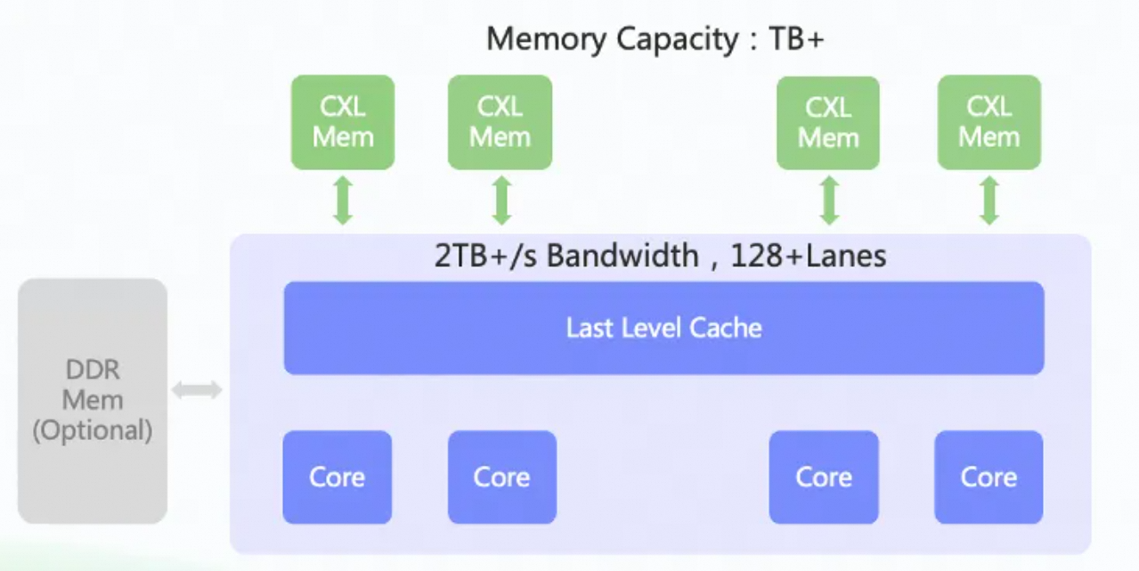
Figure: CPU memory structure reconstructed by using CXL serialized memory
AI models bring technical and engineering challenges to the design and implementation of servers, and also create more opportunities. Supernode servers emerge as the times require. Both supernode AI servers and general-purpose computing supernode servers are designed to provide higher-density computing, cache, and I/O resources, making local parallel computing faster and more efficient. The biggest change between supernode servers and traditional servers is interconnection. The differences between supernode servers and data center warehouse-scale computers lie in the interconnection scale, bandwidth, and latency.
Especially for foundation model inference scenarios, the end-to-end latency is a key element of user experience. Therefore, the bandwidth and latency of supernode interconnection are core challenges. The low-latency ALink protocol or CXL protocol, the single-stage interconnect architecture, and the limited node scale are all designed to tackle the bandwidth and latency challenges. Panjiu supernode AI servers will embrace open standards and work with industry partners to build the future of supernode servers.
Dun & Bradstreet x Alibaba Cloud: Data Intelligence + AI Drives Sustainable Business Growth
Alibaba Cloud Honored with "Open-Source AI Advancement Award" at AI EXPO Europe

1,399 posts | 492 followers
FollowFarruh - December 5, 2025
Regional Content Hub - December 15, 2025
Regional Content Hub - December 10, 2025
Regional Content Hub - December 10, 2025
Regional Content Hub - December 15, 2025
Regional Content Hub - December 22, 2025

1,399 posts | 492 followers
Follow Container Compute Service (ACS)
A cloud computing service that provides container compute resources that comply with the container specifications of Kubernetes
Learn More Container Service for Kubernetes
Alibaba Cloud Container Service for Kubernetes is a fully managed cloud container management service that supports native Kubernetes and integrates with other Alibaba Cloud products.
Learn More Apsara Stack
Apsara Stack is a full-stack cloud solution created by Alibaba Cloud for medium- and large-size enterprise-class customers.
Learn More Tongyi Qianwen (Qwen)
Top-performance foundation models from Alibaba Cloud
Learn MoreMore Posts by Alibaba Cloud Community